Common clocking errors with 7-Series FPGAs
This is a list of the most common errors I have seen users make when creating clock structures in 7-Series devices. Most of this list applies to both the MMCM and the PLL.
Not reading the documentation
You can't design effectively and efficiently if you don't know how to use the target device. Read the device family documentation, then read the Clocking Guidelines
section in the UltraFast Design Methodology Guide - search the Xilinx website for UG949.
Then read them again.
Clock Buffer between clock input and MMCM
I've lost count of the number of times I've seen a BUFG stuck between the clock input pads and an MMCM (or PLL). You
just don't need it...well, mostly. If you have logic and an MMCM connected to the external clock then it might be necessary.
But in this case ask yourself if it's not possible to move the BUFG and logic to one of the outputs of the MMCM rather then the input.
If there's no logic on the input side of the MMCM, then eliminate the buffer completely and connect the IBUFG (or IBUFGDS) directly to
the MMCM input. Note that if you have already completed designs with this error, there is no need to rush off and change them - nothing "bad" will happen.
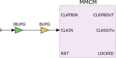
Figure 1: Buffer on external clock input
Unecessary buffer in MMCM feedback loop
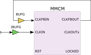
Figure 2: Unecessary buffer in feedback loop
Another classic..the useless BUFG inside the MMCM feedback loop.
This buffer is only required if you need clock deskewing, that is a known, fixed phase relationship
between the MMCM input clock and the MMCM output clock(s). Clock deskew is also known as phase alignment.
The reason this problem crops up often is because the Clocking Wizard in Vivado has the Phase Alignment option enabled
by default.
Again, nothing bad will happen to your design if you include this buffer in the feedback loop, but if all you need is frequency synthesis
then you're wasting a clock buffer.
Allowing the logic to be clocked before LOCKED goes active
The LOCKED output of the MMCM indicates that the output clock are valid and can be safely used - before LOCKED goes high, the output
clocks are not guaranteed to be stable. If you don't hold your logic in a known state, usually with a reset, then you risk it occasionally starting up
incorrectly - one of the most difficult hardware problems to debug.
There are at least two ways to solve this problem:
1. Use the safe start option in the Clocking Wizard
The 7-Series Clocking Wizard in the Vivado tool suite has an option called Safe Clock Startup. When this option is selected, the wizard will automatically add a shift register that disables the clock buffers on the MMCM outputs until LOCKED is high. The only problem with this solution is that it adds an extra BUFH for every clock output - os if you have say, three MMCM output clocks, you will get three clock buffers on those outputs, plus three extra BUFH buffers to clock the shift registers.
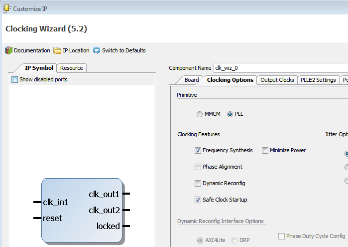
Figure 3: Safe Start option
2. Create a reset circuit based on LOCKED
My personal preference is for a reset circuit that keeps everything in reset until LOCKED goes active. Figure 4 here shows one possible configuration for this. It is based on a shift register that creates a synchronously released, active high internal reset signal. The external reset button will cause the MMCM be reset and this will set LOCKED inactive (low). The inverted version of LOCKED then asynchronously presets the shift register such that all flip-flops have their Q output set high and the Internal Reset signal is now active. Once LOCKED goes active high, the shift register starts to clock the logic '0' at the D input of the first stage until the Internal Reset signal goes low (inactive). Note how the Internal Reset signal is activated asynchronously, but released synchronously to the clock.
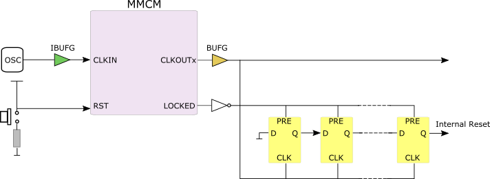
Figure 4: Reset circuit using LOCKED
Changing the length of the shift register will change the time that Internal Reset is active after LOCKED goes high. If you have a multi-clock domain design with asynchronous clocks (..and doesn't everyone?..) then you will probably need one of these circuits for every asynchronous clock domain.
Using an MMCM for simple clock divisions
Sometimes it's better to avoid using an MMCM or PLL completely if the clock division factors are simple integers. An MMCM is not the most "power-lite" feature in today's FPGAs. There are other alternatives to creating a series of clocks that are divided down from a single master clock. For example, if you need to create circuits that run at 100MHz, 50MHz and 25MHz starting from a 200MHz master clock, the most obvious solution seems to be an MMCM which divides by 2, 4 and 8. However, it might be better to use a single 200MHz clock tree and three clock enables that have periods of 100, 50 and 25MHz. For more details on using SRLs to divide down clocks, see this article.
Unbuffered clock nets
Not every clock net needs a buffer, but if there are many loads and skew is important (..and it usually is..) then make sure the clock net has a
clock buffer of some sort.
Vivado has a powerful search facility and it can help you find what it calls local clocks, nets that go to the clock pins of one or more synchronous elements
but are not buffered in any way. Just open the synthesized or implement design, then search like this:
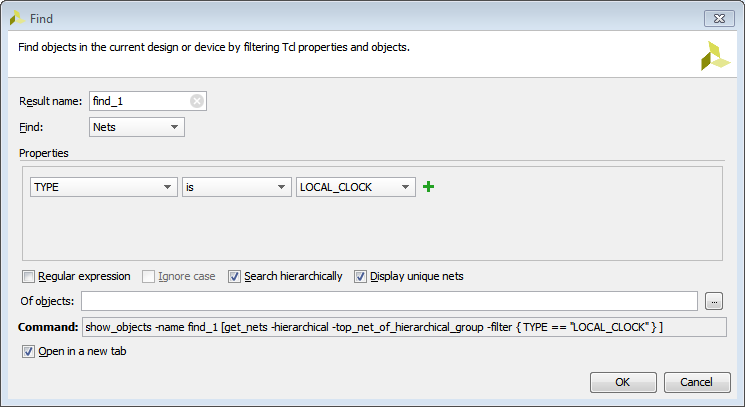
Figure 5: Finding local clocks with Vivado search
You can ignore any nets that have a falt pin count of just 2, this means that they go to just one clock pin and so skew will not be an issue.
Anything with a flat pin count higher than 2 should be evaluated to see if really should have a clock buffer or not.
To see how the net is connected in schematic form, just select it in the search results list and then hit F4.
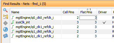
Figure 6: Search results showing flat pin count
Not checking for Cross-Clock Domain paths
Paths that cross from one asynchronous domain to another can be dangerous to the health or your design..and they are easy to miss. Vivado now has a Cross-Clock Domain (CDC) checker that will report paths that start in one clock domains and pass into another. To run it, select Tools -> Report -> Timing -> Report CDC from the GUI menus, or run the tcl command with the required options, a bit like this:
- report_cdc -file cdc_sign_off.txt
The CDC report can be generated either in graphical form inside the Vivado GUI, or as a text file which can be submitted as part of the sign-off procedure...and if CDC checking isn't part of your sign-off, then you're potential missing something that could come back and bite you later on.
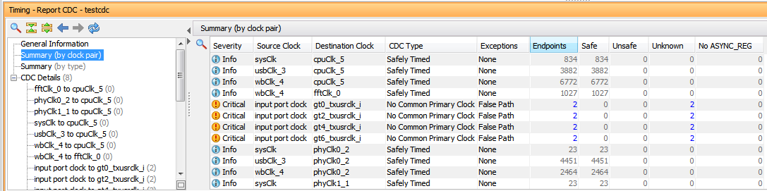
Figure 7: CDC checker results